
Equipment Manufacturing Products

- Complete erasing of charges of EPROM and Flash memory.
- UV Curing and Hardening.
- Removal of stress induce due to manufacturing processes. Features :
- Flexible to handle 150mm and 200mm wafers without conversion
- Class 1000 cleanliness
- Multi wafers UV chamber for high throughput
- Low cost of ownership
- Wafer robot handling
- Cassette to Cassette Transfer
- Wafer aligner & OCR (Option)
WAFER UV ERASER SYSTEM I ( AER681 / AER682 )
Applications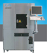
Click on image to view brochure
- Complete erasing of charges of EPROM and Flash memory.
- UV Curing and Hardening.
- Removal of stress induce due to manufacturing processes. Features :
- 300mm ready
- Class 10 cleanliness
- Modular design for future expansion
- Capable of handling thin wafer
- GEM full compliance
- Wafer sort - FOUP to FOUP or FOUP to FOSB
WAFER UV ERASER SYSTEM II ( AER8121 )
Applications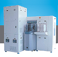
Click on image to view brochure
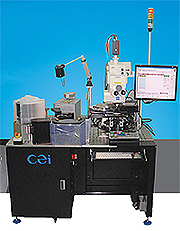
- Wafer Sorting.
- Optical inspection with Inkless Binning. Features :
- Atmospheric robot wafer handling
- Capability to handle thin wafer (>6 mils)
- Multi function- Cassette to Cassette Sort , Cassette to XY-stage for micro inspection
- Inkless Binning catered to handle all Semi Std Map Format
- Macro inspection (Frontside , Backside & Edge defect)
- Tilting & Spin Module
- Capable to integrate with any OEM Microscope
- Optical Character Reader (OCR)
- Smallest foot print
- SEC II GEM (Option)
- Wafer Aligner (Option)
MACRO AND MICRO OPTICAL WAFER INSPECTION SYSTEM
( AWL681 / AWLM681 )
Applications
Click on image to view brochure
- Wafer sorting/packing & unpacking Features :
- Flexible to handle wafer from 120mm, 150mm & 200mm
- Thin wafer handling capability down to 6 mils
- SEC/GEM full compliance
- Enable full wafer integrity and traceability
- Eliminate human handling
- Reduces wafer loss and improve yield
- Safe, automated environment
- Macro inspection (Frontside, Backside & Edge defect)
WAFER SORTING SYSTEM ( BTC681 )
Applications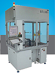
Click on image to view brochure
- Wafer sorting / packing & unpacking Features :
- 300mm ready
- Class 10 cleanliness
- Modular design for future expansion
- Capable of handling thin wafer
- GEM full compliance
- Enable full wafer integrity and traceability
- Eliminate human handling
- Reduces wafer loss and improve yield
- Safe, automated environment
WAFER SORTING SYSTEM ( BTC8121 )
Applications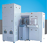
Click on image to view brochure
- 3rd Optical Inspection Machine with auto conversion Features :
- Flexible to handle both lead frame & substrate
- One touch auto conversion
- Strip mapping for reject traceability
- Reject Identification (Wire breaker/inking/scribing)
- Fine pitch capability for 1x1mm device
- Angular tilting mechanism to check bonding quality
- SEMI/CE compliance
- Networking capability - SECS/GEM
- 2D vision inspection for Wire & Die
OPTICAL INSPECTION MACHINE ( OPT653(V) )
Applications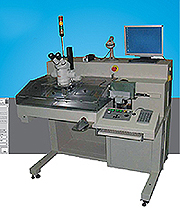
Click on image to view brochure
- We will design or custom-build our clients panels to comply with UL 508A requirements
- We will maintain component documentation necessary to prove compliance
- We will work closely with our clients to address specific constructions or components used to ensure compliance with UL 508A
CEI Limited is a Listed
UL 508A Industrial Control Panels Manufacturer
Our Value Commitment to our Client
Click on image to view brochure